1. History of DMD
Digital Mirror Device, or DMD for short, is the core device of Texas Instruments’ Digital Light Processing Technology (DLP). The original idea of DMD came out in 1977 by a TI Fellow at Texas Instruments named Larry J. Hornbeck, who right now is an elected member of the National Academy of Engineering.
Although the official short name of DMD was already used at the beginning, the full English name is not exactly the same as it is now. Because of the technological limitations, digital technology had not developed yet. Engineers used analog technology to drive the micromirrors on the chips, and the reflective surface was made of a flexible material. Due to that, the full English name of DMD at that time was called “Deformable Mirror Device”1.
Deformable mirror device is made of a combination of many units, each unit has its own independent controller which can control the voltage. Under the control of the applied voltage, the surface shape of the mirror can be modified. Different shape of the mirror can change the optical path of the optical light wave or the refractive index of the transmission medium, and change the phase structure of the incident optical light wave, so as to correct the phase of the optical light wave.
In 1987, Dr.Hornbeck officially developed a new generation of DMD devices with digital control technology and changed the full name to “Digital Mirror Device”. In the early days of the birth of digitally controlled DMD, it has developed in two different directions: printing technology and digital imaging. By 1992, Texas Instruments invested in the establishment of a digital imaging division to explore the possibility of DMD in commercial applications.
In 1994, the first prototype DLP projector developed by DMD for demonstration was born. In the April of 1996, the first commercial DLP projector based on DMD was officially born. In 1997, Texas Instruments terminated its research and development in printing technology and devoted itself to the research of digital imaging technology. Since then, DMD has developed at an amazing rate. In 2001, Texas Instruments announced the birth of its 1 millionth DMD chips since 1996.
2. Modelling and Design
2.1 DLP
Before introducing the modeling and design of DMD, it is necessary to introduce its basic technical principle and Digital Light Processing (DLP).2
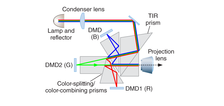
Digital light processing is commonly used in projection display technology. Today, DMD is an important MEMS device in DLP. One of the working principles of DLP is shown in the figure 2. The lamp and reflector emit light sources combined by three basic colors which red, green and blue. And then the light sources are condensed by a condenser lens, so that the light does not diverge and reducing the loss of light.
By introducing the light path into the TIR prism through a mirror, the light enter the light processing system. Then, By using the color-splitting prisms, three light sources whose colors are red, green, and blue are separated according to their wavelengths. Three channels of light are separated. They are independent red light source, green light source and blue light source. The three channels of light will be hit on the corresponding DMD.
Two things will happen at this time. When the DMD is in the “on” position, the micromirror will reflect the light hitting it to the optical output port. When the DMD is in the “off” position, the micromirror reflects the light hitting it onto an absorbing surface which can completely absorbs the light.
Light sources that are not absorbed will pass through color-combining prisms, which will fuse these light sources into one light path. Finally, this light path is projected onto the screen after passing through the projection lens.
From the entire process, we can see that the core of DLP technology is to control the DMD. By controlling the state of the DMD, we can control the color of the output light, and then change the projected image.
2.2 Modelling of DMD
In the previous section, we discussed how DLP works. Here we find that the role of the core device DMD is to reflect the corresponding light to different places under controlled conditions. Firstly, it requires that the DMD can be controlled artificially, by electricity or other signals. Secondly, it controls a mirror that can reflect as much light as possible. Moreover, since a DMD is actually equivalent to a pixel on the screen, it needs to be small enough to make the projected image more detailed. Finally, if it is used for film projection, the DMD needs to have a fast response speed. These conditions determine the modeling of DMD.
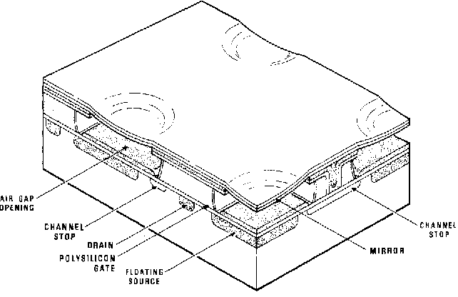
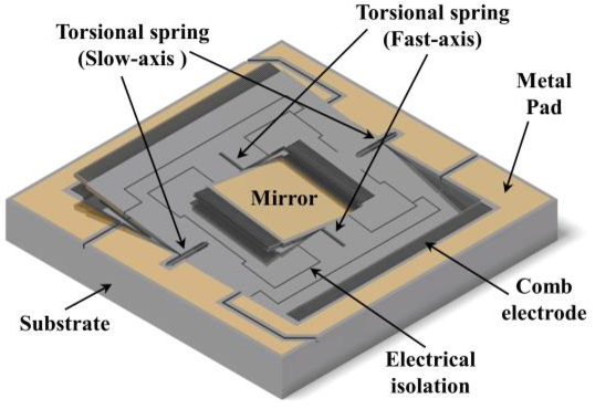
DMD is mainly composed of CMOS SRAM Substrate, Hinge, Yoke, Mirror and three electrodes, as shown in Figure 3. The area of a single DMD unit is approximately 16 μm × 16 μm.
CMOS SRAM as the base of the entire DMD unit is at the lowest level. On the substrate is a metal layer used as electrodes. There are two types of electrodes: reset electrode and address electrode. The reset electrode is connected to hinge. The two address electrodes are respectively distributed in two directions of mirror deflection. The top layer is the mechanical structure part of DMD, which is composed of Hinge, Yoke and Mirror. The mirror is fixed on the yoke. The hinge fixed on the pillar can drive the yoke to rotate, and then make the reflector to deflect.
There are two cases of the deflection angle of the micromirror. When the DMD is “on” or “off” respectively, the deflection angle of the micromirror is +10 degrees or -10 degrees. The switching time from full “on” state to full “off” state is less than 20 μs.3
With this structure, the area of the micromirror can be maximized, covering almost the entire unit. This can improve the imaging quality of brightness.
2.3 Controlling of DMD
CMOS SRAM is used to store 0 or 1 data. Based on these data, the state of DMD is determined, and then the deflection direction of the micromirror is controlled.
The reset electrode is directly powered by an external drive circuit. Its role is to reduce the voltage required to drive the corner of the micromirror. When the signal voltage and the reset voltage are applied to the address electrodes together, electrostatic attraction is generated between the micromirror and the address electrodes. The mirror will tilt until the electric potential between the poles reaches equilibrium. This achieves the deflection of the mirror surface.
3. Challenges and Development of Microfabrication Process
3.1 Microfabrication Process of DMD
In the microfabrication process of DMD, the biggest difficulty lies in how to complete the mechanical structure of hinge. Because DMD is a micron-level device, and the response time of DMD is also in the microsecond level, it is a great challenge to create a hinge that can rotate flexibly on it.
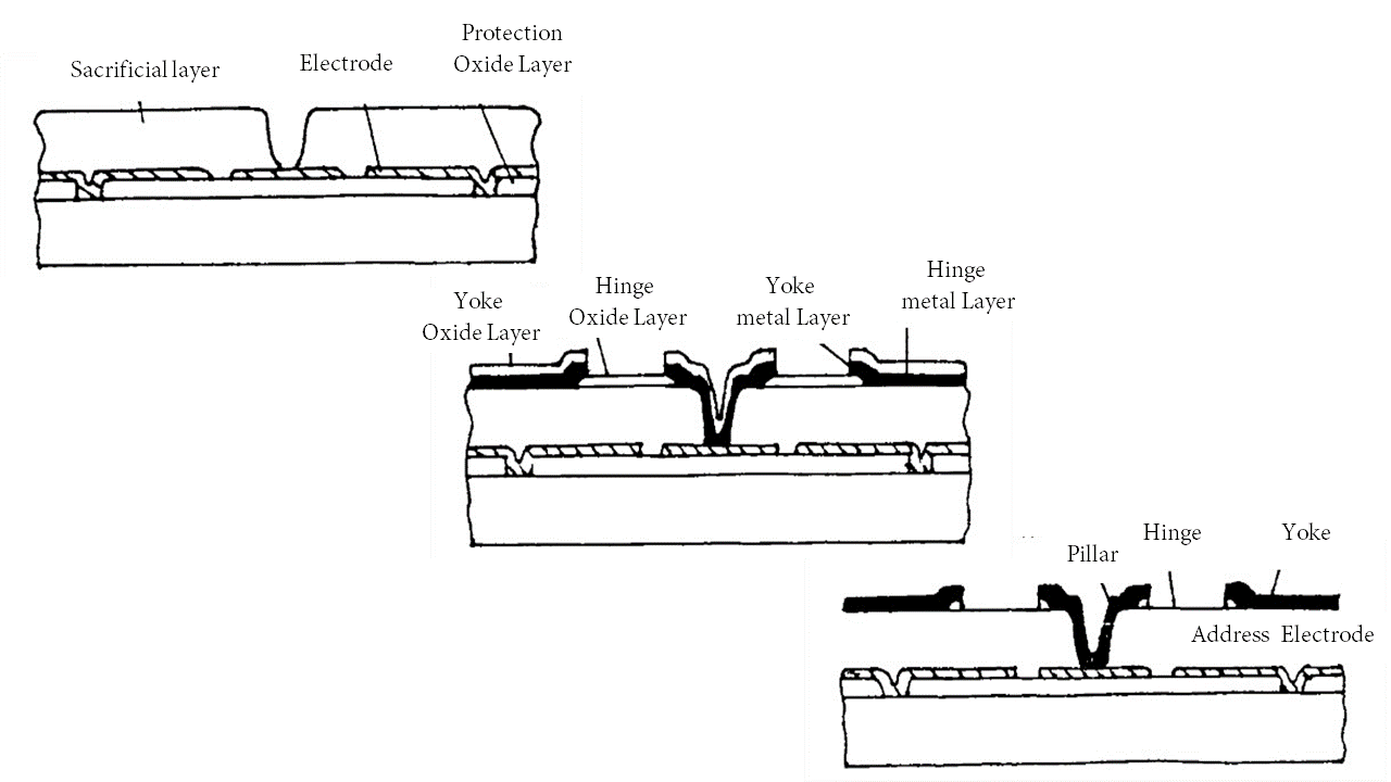
Figure 4 shows the microfabrication process of DMD. The first step is to have a CMOS SRAM as the substrate of the entire device. This SRAM silicon wafer is processed by chemical mechanical polishing (CMP). This way can flatten the wafer surface and provide a flat base for the entire DMD to ensure the stability and normal operation of the superstructure.
The next step is making the electrode. At first, cover the substrate with a protective oxide layer. Then, etch holes for connecting the SRAM and the electrode. Finally, deposit a layer of metal as electrode by electron beam evaporation. The metal is usually aluminum.
The following is the most critical mechanical structure. Covering a sacrificial layer. Then use X-Ray lithography to create a deep hole. Aluminum pillars are made in the place of the hole by metal deposition.
Sputter a thin layer of aluminum on the surface, and deposit an oxide layer directly on it. This a thin layer of aluminum will be made into a hinge, so the pattern of the hinge should be carved on the oxide layer and used the oxide as a mask. Then a thick layer of aluminum is sputtered, and an oxide layer is also directly deposited on it. This layer of thick aluminum will be made into yoke, so the pattern of the yoke should be carved on this oxide layer.
Then, etch the excess aluminum by ion washing. Because of the protection of the oxide layer, the aluminum of yoke and hinge will not be etched. Then the oxide layer is etched away, and the mechanical structure is done right now. Doing so ensures a reliable connection between hinge and yoke.
Then, a layer of sacrificial layer was coated on the surface by spin-coating and then a layer of aluminum was sputtered on it. This layer of aluminum will act as a reflective micromirror.
Finally, remove all the sacrificial layers, and the structure of the entire DMD is completed.
3.2 Development of Microfabrication Process
In recent years, flip-chip technology is also used to package DMDs. The key step is to interconnect the bare chip to the substrate using the conductive adhesive bonding method in flip-chip soldering technology.4
After depositing the masking layer, the metal layer alignment and pads are etched by photolithography after undercoating. Deposit the passivation layer, the substrate will be finished after the passivation layer is opened. Grow the bumps on the bare chip, and the bare chip is interconnected to the substrate by a conductive adhesive bonding method. At this point, the package design is complete.
This microfabrication process improves devices responsiveness, optimizes layer structure, improves electrical performance, and completes the design process of packaging substrate.
4. DMD Engineering Applications
In Chapter 2, we mentioned the use of DMD in DLP. This was also the original purpose of DMD’s invention. At that time DMD was mainly used for projection equipment. The use of DMD in DLP results in a larger projection area, better picture quality, and faster image refresh. Until today, most projection instruments use DMD as the projection driver.
In engineering applications, there is also a place for DMD.
In the previous sections, it is not difficult to see that the essence of DMD is its ability to quickly control very small pixels of light. Its two biggest features are its rapid response and small control unit. Therefore, in engineering applications, DMD will be used in digital lithography.
There are currently four types of digital lithography based on spatial light modulation devices, namely DMD based digital lithography, LCD (Liquid Crystal Display) based digital lithography, LCoS (Liquid Crystal on Silicon) based digital lithography and LBS (Laser Beam Scanning) based digital lithography.
In the field of micromachining using DMD based digital lithography system, there are two main research hotspots: grayscale lithography and micro-stereo lithography. These two technologies use different image processing and control methods to achieve the processing of specific targets, but both use the DMD as the core device.
Grayscale lithography uses a binary pulse width modulation (PWM) method to control the angle and time of microscope flip in DMD. The different flip angles and times of the microscope are equivalent to different lithography intensities. The use of this technology allows for increasing lithographic efficiency and the processing of complex continuous surface shapes. It is now possible to process 1μm lines using grayscale lithography.56
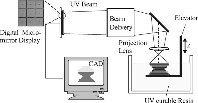
Micro-stereo lithography is used for the microfabrication of three-dimensional structures, which in simple terms is 3D printing. The software splits the 3D model into a series of bitmaps in cross-section. The DMD is then controlled to generate the corresponding dynamic digital masks based on the bitmap of each layer. Light is projected through the mask onto the surface of the liquid resin, which is light-cured to form a shape of a certain thickness. Shape of the bitmaps figure can be completed one by one, and then the entire 3D structure is created. Nowadays, it is possible to process 0.6μm lines using micro-stereo lithography.7
5. Compare with Other MEMS Devices
In the previous chapter, I mentioned four digital lithography techniques. In addition to the DMD based digital lithography technology detailed, there are three other digital lithography technologies based on LCD, LCoS and LBS devices.
Since the essence of LCD device is to control space light using the directional properties of liquid crystal molecules, it is not a MEMS device. So it will not be compared here.
5.1 LCoS Device
LCoS device is very similar to LCD device. The LCD directly uses the molecular properties of the liquid crystal to control the spatial light that passes through it. But LCoS is different from it. LCoS uses a single piece of CMOS as a substrate which is smoothed and coated with aluminum as a reflector. The liquid crystal is injected and packaged between the CMOS substrate and the glass substrate. In use, the light source is injected from outside, passes through the liquid crystal, and is reflected by the CMOS reflector. Spatial light is processed by a CMOS-controlled liquid crystal. Therefore LCoS is a reflective device.
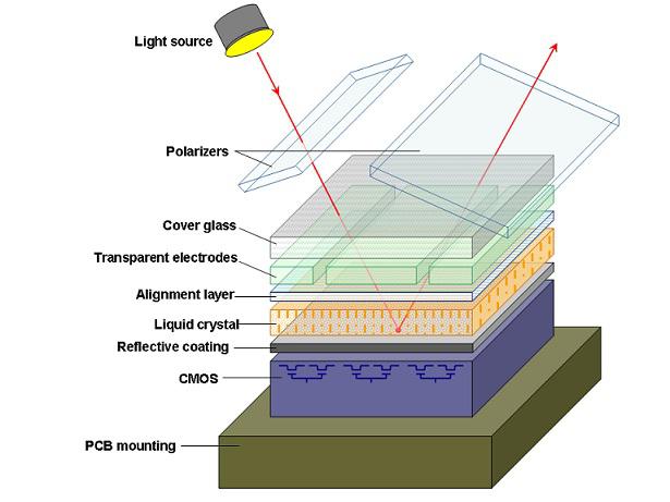
Based on the principle of LCoS, it can be easily discovered that it is actually the circuit on the CMOS that drives the liquid crystal to change the light source. It will also be limited by liquid crystal performance, so LCoS devices will have much slower response times than DMD, just like LCD devices. Since the light source needs to pass through the liquid crystal twice, the light energy is lost. The optical efficiency, contrast and brightness of LCoS will be much worse than that of DMD, which can directly reflect the light source.
Otherwise, The layered structure of LCoS devices is quite complex, increasing its manufacturing cost. Moreover, liquid crystal is highly influenced by temperature, which will be easily lead by prolonged light exposure, so LCoS performance will be degraded for prolonged operation and the chip life is short. DMD’s relatively simple mechanical structure provides lower manufacturing costs and longer chip life.
5.2 LBS Device
LBS is a technology proposed by Microvision, using in their product called PicoP. Its core device is the MEMS scanning mirror.8
MEMS scanning mirrors control light by reflecting specific light into specific locations, as does DMD. However, MEMS scanners are not controlled in the same way in microscopes, which are magnetically controlled by electrodes from both horizontal and vertical directions. Therefore, the deflection angle of the MEMS scanning mirror is controlled and the degree of freedom is two-dimensional.
In addition, the lasers used in PicoP are not the same as traditional continuous lasers. It uses a laser that outputs a high-frequency laser pulse, which means its laser is switchable.
LBS achieves light projection by coordinating the control of MEMS scanning mirrors and lasers.
Since LBS needs to produce high frequency lasers, the power used is very high, which limits the speed at which lasers can be switched on and off. lasers in DMD do not need to be switched on and off, so they will have a better display. However, it is precisely because the lasers in the DMD cannot be switched on and off that the DMD can only deflect and absorb light when it is not needed, generating a lot of excess power and heat during this time. This is also the reason why most of the DLP products on the market have serious heating problems. LBS will not have this problem.
Otherwise, MEMS scanning mirror has two-dimensional degree of freedom, so only one MEMS scanning mirror is needed to achieve a certain range of scanning projection. However, a DMD can only implement projection of one single pixel point, which means that a series of DMDs are needed to implement a certain range of projections.
6. Summary and Outlooks
This report reviews the history of the DMD and learns about this tiny device that was invented by the whims of Larry J. Hornbeck. Then the principle of DLP system is explained, and the structural modeling of DMD and its control method are derived from the working principle. This is followed by a brief description of its microfabrication process and some current improvements based on DMD’s modeling. Finally, we discuss the advantages and disadvantages of each of the three MEMS devices, DMD, LCoS and LBS, by comparing them.
DMD technology has been evolving for over forty years to the present day. With the development of other technologies in the MEMS field, the latest generation of single DMD has been able to achieve a size of 13 μm × 13 μm.
Today, DLP equipment using DMD has taken over half of the projection field. With the rise of 3D printing technology, DMD will also experience another development boom. But technologies such as LBS can also create some competition for DMD.
In the field of projection, people are not satisfied with the current 2D projection. 3D projection has already made its debut in some venues such as concerts. This shows that in the future, making 3D projection cheaper and more accessible to the general public will be a trend. Perhaps the next generation of DMD can also feature prominently in 3D projection.
In conclusion, the application and development of DMD is not limited to the present. It still has a great development prospects.
-
Hornbeck, Larry J. “128× 128 deformable mirror device.” IEEE Transactions on Electron Devices 30.5 (1983): 539-545. ↩
-
Hornbeck, Larry J. “Digital light processing and MEMS: An overview.” Digest IEEE/Leos 1996 Summer Topical Meeting. Advanced Applications of Lasers in Materials and Processing. IEEE, 1996. ↩
-
Yoder, Lars A. “The Fundamentals of Using the Digital Micromirror Device (DMD (TM)) for Projection Display.” (1995). ↩
-
Zhongnan, Li , and W. Shuxian . “Design of the Flip-Chip Package for Digital Micromirror Devices.” semiconductor technology (2012). ↩
-
Ljungblad, Ulric , et al. “A High-End Mask Writer using a Spatial Light Modulator.” Proceedings of Spie the International Society for Optical Engineering 5721(2005). ↩
-
Chan, Kin Foong , et al. “High-resolution maskless lithography.” Journal of Micro/nanolithography Mems & Moems 2(2003). ↩
-
Sun, C. , et al. “Projection micro-stereolithography using digital micro-mirror dynamic mask.” Sensors & Actuators A 121.1(2005):113-120. ↩
-
Gurevich, B. S. . “Laser projection displays based on acoustooptic devices.” Journal of Optical Technology C/c of Opticheskii Zhurnal 70.7(2003):500-503. ↩